The VSDSquadron FPGA Mini (FM) board features the Lattice ICE40UP5K FPGA with the following capabilities:
- 48-lead QFN package
- 5.3K LUTs for flexible logic design
- 1Mb SPRAM and 120Kb DPRAM for efficient memory usage
- Onboard FTDI FT232H USB-to-SPI interface for programming and communication
- All 32 FPGA GPIO accessible for rapid prototyping
- Integrated 4MB SPI flash for configuration and data storage
- RGB LED for user-defined signaling
- Onboard 3.3V and 1.2V power regulators, with the ability to supply 3.3V externally
The following illustration in Figure 2 highlights various components of the VSDSquadron FPGA Mini (FM) board.
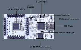
Figure 2: VSDSquadron FPGA Mini (FM) board
Form Factor
The following are the dimensions of the VSDSquadron FPGA Mini (FM) board.
- Form factor is 57.00 x 29.00 mm
- Maximum height of the component at the top side: 8mm
- Maximum height of the component at the bottom side: 1mm
| FNC | Pin Type | BANK | Differential Pair | Pin number |
| IOB 0a | PIO | 2 | – | 46 |
| IOB 2a | DPIO | 2 | TRUE of IOB 3b | 47 |
| IOB 3b G6 | DPIO/GBIN | 2 | COMP of IOB 2a | 44 |
| IOB 4a | DPIO | 2 | TRUE of IOB 5b | 48 |
| IOB 5b | DPIO | 2 | COMP of IOB 4a | 45 |
| IOB 6a | PIO | 2 | – | 2 |
| IOB 8a | DPIO | 2 | TRUE of IOB 9b | 4 |
| IOB 9b | DPIO | 2 | COMP of IOB 8a | 3 |
| IOB 10a | DPIO | 1 | TRUE of IOB 11b | – |
| IOB 11b G5 | DPIO/GBIN | 1 | COMP of IOB 10a | – |
| creset b | CONFIG | 1 | – | 8 |
| IOB 12a G4 CDONE | CONFIG/DPIO/GBIN | 1 | TRUE of IOB 13b | – |
| CDONE | CONFIG | 1 | – | 7 |
| IOB 13b | DPIO | 1 | COMP of IOB 12a | 6 |
| IOB 16a | PIO | 1 | – | 9 |
| IOB 18a | PIO | 1 | – | 10 |
| IOB 20a | PIO | 1 | – | 11 |
| IOB 22a | DPIO | 1 | TRUE of IOB 23b | 12 |
| IOB 23b | DPIO | 1 | COMP of IOB 22a | 21 |
| IOB 24a | DPIO | 1 | TRUE of IOB 25b | 13 |
| IOB 25b G3 | DPIO/GBIN | 1 | COMP of IOB 24a | 20 |
| IOB 29b | PIO | 1 | – | 19 |
| IOB 31b | PIO | 1 | – | 18 |
| IOB 32a SPI SO | DPIO/CONFIG SPI | 1 | – | 14 |
| IOB 33b SPI SI | DPIO/CONFIG SPI | 1 | – | 17 |
| IOB 34a SPI SCK | DPIO/CONFIG SPI | 1 | – | 15 |
| IOB 35b SPI SS | DPIO/CONFIG SPI | 1 | – | 16 |
| VCCPLL | VCCPLL | – | – | 29 |
| IOT 36b | DPIO/I3C | 0 | COMP of IOT 37a | 25 |
| IOT 37a | DPIO/I3C | 0 | TRUE of IOT 36b | 23 |
| IOT 38b | DPIO | 0 | COMP of IOT 39a | 27 |
| IOT 39a | DPIO | 0 | TRUE of IOT 38b | 26 |
| IOT 41a | PIO | 0 | – | 28 |
| IOT 42b | DPIO | 0 | COMP of IOT 43a | 31 |
| IOT 43a | DPIO | 0 | TRUE of IOT 42b | 32 |
| IOT 44b | DPIO | 0 | COMP of IOT 45a | 34 |
| IOT 45a G1 | DPIO/GBIN | 0 | TRUE of IOT 44b | 37 |
| IOT 46b G0 | DPIO/GBIN | 0 | – | 35 |
| IOT 47a | PIO | 0 | – | – |
| IOT 48b | DPIO | 0 | COMP of IOT 49a | 36 |
| IOT 49a | DPIO | 0 | TRUE of IOT 48b | 43 |
| IOT 50b | DPIO | 0 | COMP of IOT 51a | 38 |
| IOT 51a | DPIO | 0 | TRUE of IOT 50b | 42 |
| RGB2 | LED | 0 | – | 41 |
| RGB1 | LED | 0 | – | 40 |
| RGB0 | LED | 0 | – | 39 |
| GND | GND | GND | – | Paddle |
| GND | GND | GND | – | Paddle |
| GND | GND | GND | – | Paddle |
| VCC | VCC | VCC | – | 5 |
| VCC | VCC | VCC | – | 30 |
| VCCIO 0 | VCCIO | 0 | – | 33 |
| SPI Vccio1 | VCCIO | 1 | – | 22 |
| VCCIO 2 | VCCIO | 2 | – | 1 |
| VPP 2V5 | VPP | VPP | – | 24 |
Table 2: ICE40UP5K-SG48ITR FPGA device IO Bank Assignment
Table 2 shows ICE40UP5K-SG48ITR FPGA device IO Bank Assignment for
communication Interfaces
The following table 3 lists the important components of the VSDSquadron
FPGA Mini (FM) board
| Feature | ICE40UP5K-SG48ITR Specification |
| Technology Node | 40 nm |
| Logic Cells | 5,280 |
| Flip-Flops | 4,960 |
| SRAM Blocks | 120 kbits |
| DSP Blocks | None |
| Package Type | SG48 |
| I/O Pins | 39 |
| I/O Standards Supported | LVCMOS, LVDS |
| Maximum Operating Frequency | 133 MHz |
| Clock Sources | Internal oscillator and external clock |
| Core Voltage | 1.2V |
| I/O Voltage | 3.3V, 2.5V, 1.8V |
| Operating Temperature Range | -40 C to 85 C |
| Development Tools | Project Icestorm, Yosys, and NextPNR tools |
Table 3: ICE40UP5K-SG48ITR FPGA Specifications
