Kunal Ghosh, the visionary co-founder of VLSI System Design (VSD) Corp. Pvt. Ltd., stands at the forefront of online open-source EDA and hardware design education, particularly in the realm of RISC-V.
With a portfolio of 50 top-tier VLSI online courses, Kunal has enriched the learning journey of over 90,000 students across 153 countries. His expertise extends beyond training; he’s actively involved in pioneering open-source projects and design collaborations with esteemed institutions like IIT Madras, IIT Bombay, IIT Guwahati and IIT Hyderabad.
His current focus is on crafting high-quality open-source Analog/Digital IPs, a groundbreaking endeavor in open-source hardware design. Kunal’s rich industry experience includes roles at Qualcomm and Cadence, specializing in SoC design. He holds a master’s degree from IIT Bombay, where he specialized in VLSI & Nano-electronics, with a focus on sub-100nm Electron Beam Lithography Optimization techniques.

Timothy Edwards, the mastermind behind Opencircuitdesign.com and the Senior Vice President at Efabless, is a seasoned Analog VLSI designer with over 32 years of dedication to developing open-source EDA tools. His career journey has taken him through notable organizations such as Johns Hopkins Applied Physics Lab, startups MultiGiG, and Analog Devices. Timothy is the brain behind renowned open-source EDA software tools like Magic, Qflow, Netgen, and Xcircuit.

Professor Mohammed Shalan of the American University in Cairo is not only an academic but also a trailblazer in the field of digital ASIC/FPGA design, evidenced by his founding of CloudV.io and Fault. His professional repertoire includes roles in embedded systems architecture for the automotive and mobile sectors at Mentor Graphics, as well as positions at MindSpeed, Freescale, and as a SoC consultant. Mohammed is a patent holder in Power Profiling and Optimization for Embedded System Design.
VSD Launches VSDSquadron In Collaboration With IIT Madras & DIR-V

Job Roles, Convergence With Embedded Systems, and Startups
VSD showcased at Semicon India 2023

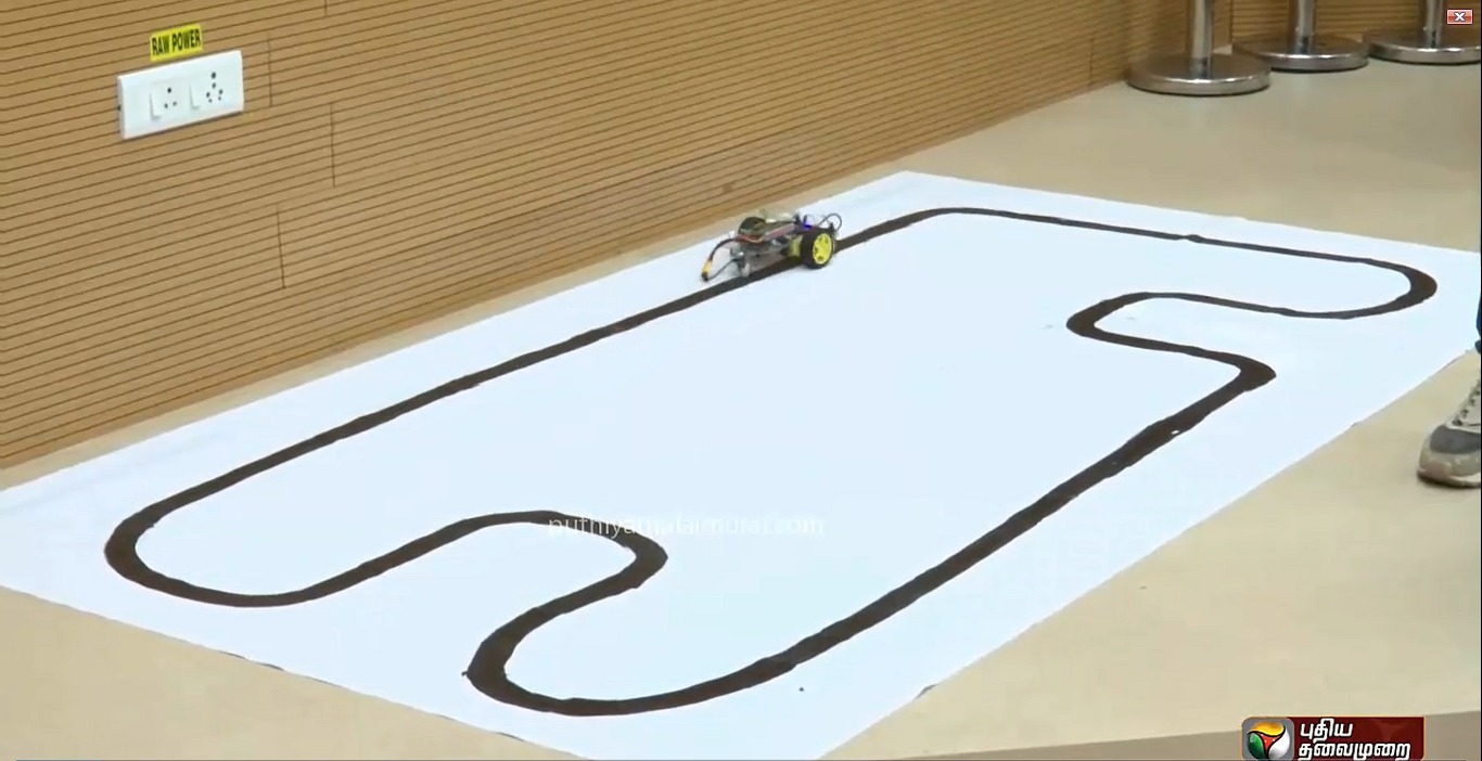
VSDSquadron Educational board on Tamil News channel
5 Day Workshop on VLSI Design Flow using RISCV and EDA Tools
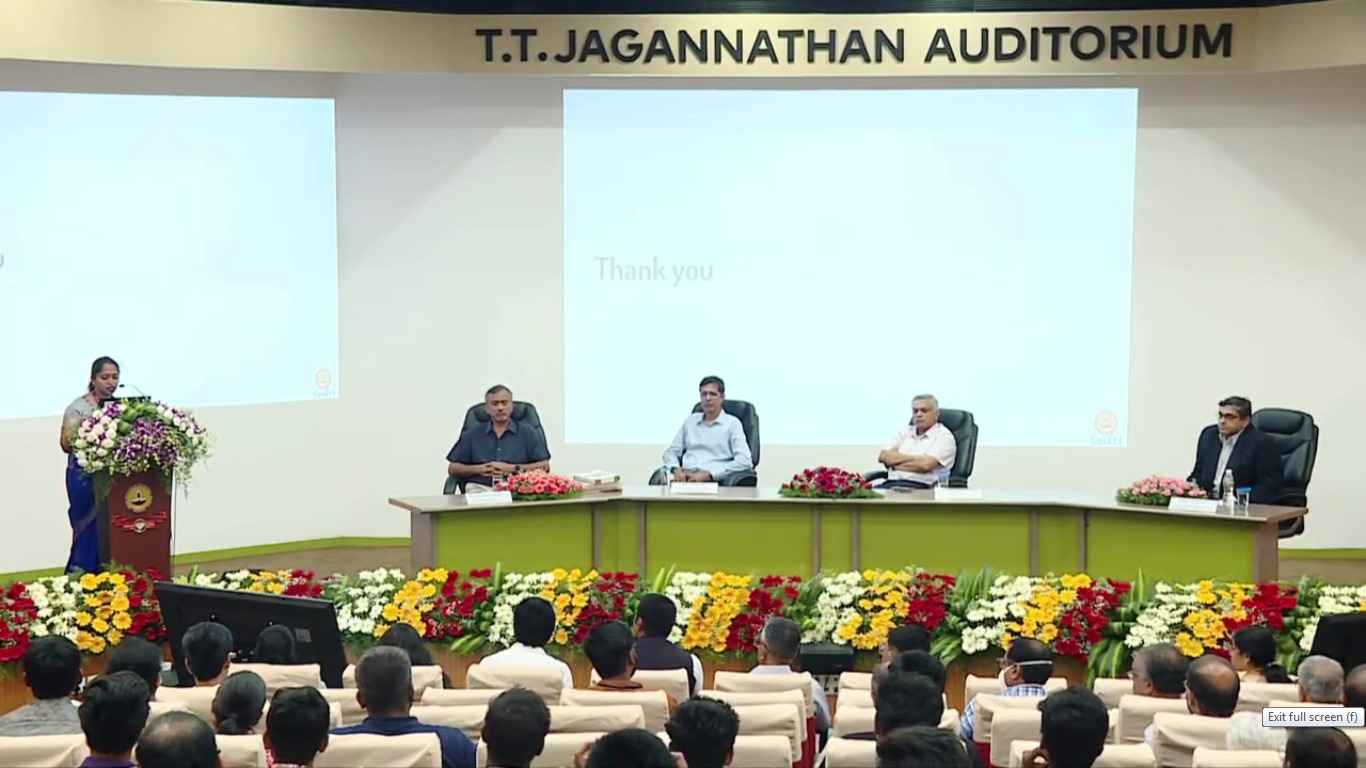
Karnataka VLSI roadshow at Sahyadri College, Mangalore
