
IP (intellectual property) as the name suggests, is a property which is a result of creativity. Ever tasted Yummy Pizzas from Pizza Hut, which was founded in 1958? Take a good look at its logo. And you would realize the amount of creativity which has gone into creating it.
For eg. Swirl shape represents tomato sauce moving in spiraling pattern. Red color is to evoke warm emotions like energy and enthusiasm which are associated with young people, their target customers. Its playful typeface represents its restaurants playful environment. Overall, the logo is in shape of thin pizza.
It really takes immense amount of focus and creativity to think of different parameters altogether and design an intuitive logo like this one. Let us talk about VSD IP design internship program
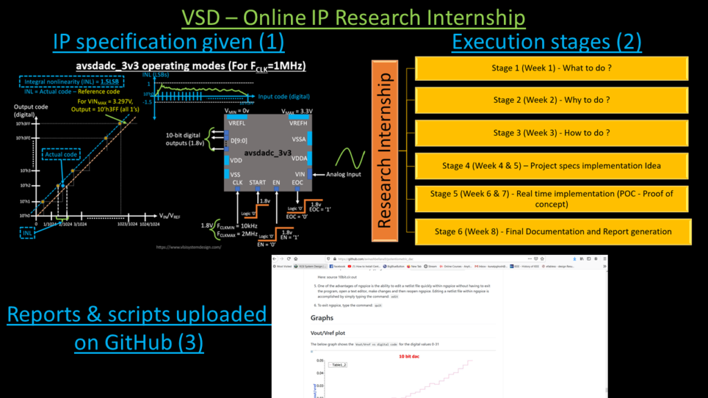
When you speak over a cell phone, your speech is in analog form and CMOS logic inside your chip understands digital. So, you would need analog to digital converter (ADC). Imagine the number of cell phones on this planet and every brand of phone will have its own set of input specifications for its own CMOS logic. Converting those input specifications in a form of custom ADC hardware using your creativity is called Intellectual Property (IP)
That is exactly what we will be doing in this internship program. You will be given a set of specifications which is remarkably close to a real application (for eg. cell phone) and you need to use your creativity to build ADC which satisfies those specifications. That is VSD 8-week IP design internship program. We will be using real CMOS logic Skywater 130nm open-source data. Which means, we are building a real ADC and not just for simulation purposes. If the ADC works and (say) some mobile phone company wants to buy the IP, just imagine the end possibilities in terms of your name and business.
Guess what – its easier said than done. And so, the IP design internship program is only for workshop participants, as the workshop will prepare you to design state-of-the-art analog IP’s and convert it into a real chip. It would need basic knowledge of VLSI, PNR tools, custom layout, STA, mixed signal and sky130 pdk’s itself, all of which is covered in 5-day workshop is a very structured fashion.
Open-source analog IP’s has been a dream of all VLSI engineers for such long time, and now with this workshop + internship, you might see that dream becoming true. This is the best opportunity, especially for freshers, who are looking forward for a career in VLSI, because not only will they learn VLSI basics, but possibly own an IP which might attract giant smartphone or electronics companies. Who knows, you might just start-up a new company around that IP?
Here is the link with more details about workshop, internship, FAQ’s, past students work on GitHub and many more (registrations closing very soon):
https://www.vlsisystemdesign.com/advanced-physical-design-using-openlane-sky130/
Get ready to work on real hard for 5days workshop + (free till now) 8-weeks analog IP design internship
All the best and happy learning
