….And this is something which I can show you using the newly launched open-source EDA tool “eSim (FOSSEE IITB Project)”.
Let’s assume for a moment, you do not have timing libraries, maybe because foundry doesn’t provide them (which is perfectly OK in terms of their business model) or maybe you are a student and don’t know from where to access them. Does that stop us from doing and learning timing analysis? Not any more….
We all have heard of sub-circuits using ngspice, but also know, it’s a bit tedious to maintain the information of subckts as its all text.
How about giving you an access to subckts using graphics, and you don’t worry about the syntax of subckts definition? Wouldn’t that be freedom? Also, that will make you analysis even more accurate than using a timing library, as you are directly using MOSFET’s to build your big digital design.
Take a look at below image (I have taken a really easy example of buffer to demonstrate the power of eSim and subckts, and how does it eliminate the need of timing libraries for small design)
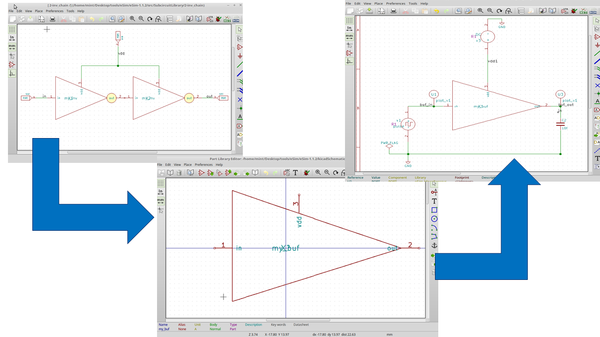
I built the small inverter shown in top left image using 180nm technology node MOSFETs in eSim. Then I created a part of the inverter and given it a shape of my choice, calling it as “my_inv”, as shown in middle image. Finally, I used “my_inv” to simulate 2-inverter chain shown in bottom right image
Now, if I am not happy with the delay of the whole inv chain, I just can tune the parameters of MOSFET’s and the whole inv-chain delay will be taken care of.
Imagine, if you had to do a basic timing analysis of the above inv-chain in a standard STA tool, you would had required timing libraries of inverter. If you had timing libraries, by any chance, you would had to simulate the inv chain using timing libraries, and use the SPICE subckts of those inverters to correlate timing between SPICE and STA tool. We really don’t need all these for a small design like above.
Now, I used the above inv-chain to build a buffer as shown below:
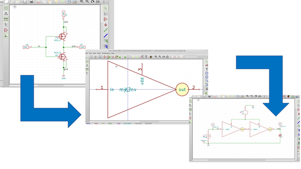
The 2-inv chain shown in top left image, represents a buffer, whose part is created by giving it proper port names and my own shape, calling it as “my_buf”as shown in bottom middle image.
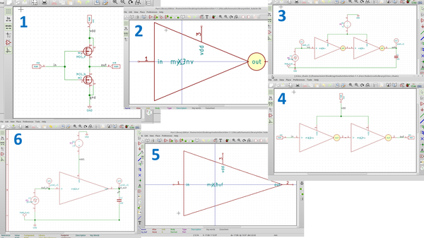
This “my_buf”part is now used to simulate a single stage buffer(You can keep on adding more buffer stages). Again, over here, if you are not happy or satisfied with your buffer delay, you can simply tune your MOSFET parameters, the changes will be propagated all along from MOSFET to INV to INV_CHAIN to BUF. It’s like a chain, where all of them are connected like below:
If you remember the vision2015 from previous blog, which me and my team had set 2 years back, you see we are very close to that, and all that happened because of constant dedication, and continuous support from IIT Bombay, one of the most prestigious institutes in India
“The future belongs to those who believe in the beauty of their dreams” – Eleanor Roosevelt
So let’s dream and own the future…
